
To make labels in KiCad, select an electrical label tool, enter the net name, and place the label’s attachment point on the intended wire or pin. Use a local label for connections within a sheet, a global label for connections across the schematic, or a hierarchical label for a defined child-to-parent sheet connection.
The instructions below explain how to make labels in KiCad using the 10.0 documentation and default shortcuts. A customized keymap can differ. The important result is an attached electrical object with the right scope, not simply a word drawn beside a wire.
Choose the label scope before placing it
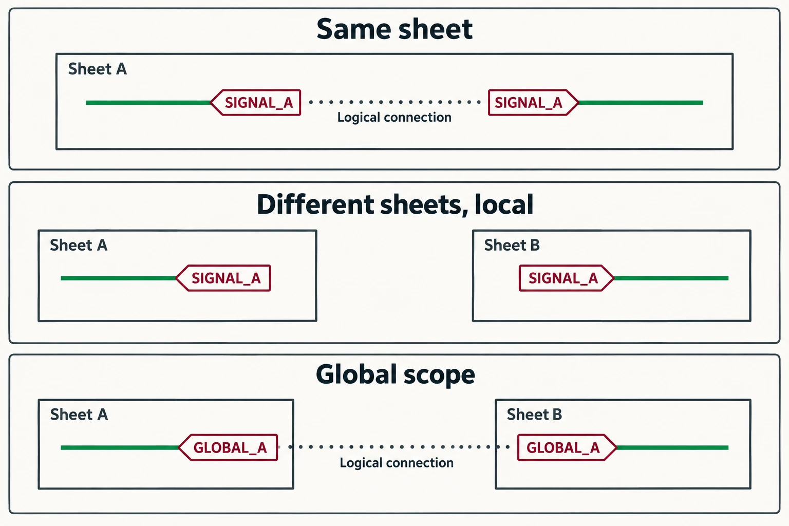
Scope determines where matching names establish a connection. Select it deliberately, especially when a design has several sheets.
| Label type | Connection scope | Typical decision |
|---|---|---|
| Local label | Matching names connect within the same sheet. | Use for a signal whose connections belong to that sheet. |
| Global label | Matching names connect across the schematic. | Use when the signal intentionally has project-wide reach. |
| Hierarchical label | Connects through the corresponding parent-sheet pin. | Use to expose an explicit interface for a subsheet. |
| Ordinary text | No electrical connection is created by the text itself. | Use for explanations and notes. |
KiCad also has directive labels for assigning classes and related properties. Do not choose a directive just because its visual appearance resembles a connectivity label. Select the tool by the electrical job you need it to perform.
How to make labels in KiCad, step by step
Create a label on a known wire first. That keeps scope and attachment easy to inspect before you use the method throughout a project.
- Open the Schematic Editor. Locate the wire or pin you intend to name. Zoom in far enough to inspect its connection point.
- Choose Place Net Labels. In the default keymap, press L. The official Getting Started guide also identifies the toolbar command.
- Enter a net name. For a simple example, use
SIGNAL_A. Choose a name that conveys the signal’s role in your project. - Attach the label. Place its connection square directly on the intended wire or pin connection point. Nearby text is not sufficient.
- Finish placement. Exit the placement tool, then inspect the label and wire together before adding more labels.
If the position is awkward, move or rotate the object while keeping the attachment correct. Do not solve a readability problem by leaving the anchor a small distance from the wire. The label can look close enough at normal zoom while still failing the intended connection.
When editing an existing label, inspect the electrical object and its name rather than adding a second text object over it. A note reading SIGNAL_A does not replace a net label named SIGNAL_A.
Verify the connection with a small exercise
Use a scratch schematic or a copy of the design for this exercise. The following is an example procedure and expected observations, not a claim that your project has been tested.
Place two separate short wires on one sheet and attach a local label named SIGNAL_A to each. Keep them visually separated so that the label connection, rather than a long drawn wire, is the point of the exercise.
Activate the Highlight Net tool on one wire. Both intended parts of the named net should highlight. If only one does, inspect the other label’s object type, spelling and attachment. Resolve those details before expanding the example.
Next, change the second label to SIGNAL_B. The two wires should now remain different nets unless some other connection joins them. If they still highlight together, inspect the rest of the schematic for a shared connection rather than assuming the rename command failed.
Finally, consider the sheet boundary. Two local labels with the same name on different sheets do not create a cross-sheet connection by themselves. Compare that intended separation with two appropriately placed global labels using the same name. This contrast is a useful way to check your understanding before editing a larger hierarchy.
Record the expected endpoints in the design review: which pins should belong to the net, and which must remain separate. Highlighting then becomes a check against an explicit intention rather than a search for any colored wire.
Global and hierarchical labels solve different problems
A global label is useful when a named connection intentionally spans the schematic. Choose the Global Label tool from the available label tools or Place menu; in KiCad 10, related tools can be grouped in a toolbar palette. Do not assume the absence of a separate visible icon means the feature is unavailable.
Place the global label’s connection point as carefully as a local label’s. Before using a common name, identify every location that should participate. A project-wide name is convenient, but it also deserves a project-wide review.
For a hierarchical interface, create the hierarchical label inside the child sheet, then add or import its matching sheet pin on the parent’s sheet symbol. Connect the parent-side circuit to that pin. Keep the names aligned; the parent sheet pin and child label form the explicit interface.
Changing a local label into another label type can change its reach. Treat that as a connectivity change, not a cosmetic cleanup. Recheck the intended endpoints after changing scope.
Active-low labels and bus names
KiCad supports overbar markup such as ~{RESET} for an active-low presentation. A project may instead use a naming convention such as RESET_N. Decide which actual net name the design uses and apply it consistently; two different names do not become equivalent because a reader interprets both as active-low.
A vector bus uses notation such as DATA[0..3], with members DATA0 through DATA3. A bus label describes a collection of signals. It does not mean those members should all be electrically shorted together.
Before adopting a bus in a larger design, list the expected individual members and verify their connections. Keep the distinction between a bundle name and a specific member name visible in both the drawing and the review notes.
Why is a KiCad label not connecting?
Check the object, scope and attachment before changing unrelated design settings.
| Observed symptom | First check | Useful confirmation |
|---|---|---|
| The name is visible but the wire stays separate. | Is it an electrical label, and is its anchor on the wire? | Inspect at close zoom and highlight the intended net. |
| Matching names do not connect across sheets. | Are they local labels? | Choose the intended global or hierarchical connection deliberately. |
| A hierarchical signal does not reach the parent. | Does the child label match the parent sheet pin? | Inspect both sides of the sheet interface. |
| A net changes unexpectedly after editing. | Did the name, scope or another connection change? | Compare actual endpoints with the design intention. |
| The schematic is correct but the PCB is stale. | Has forward annotation been applied? | Review Update PCB from Schematic and inspect the board’s net assignments. |
Check ERC and transfer the change to the PCB
Run the Electrical Rules Checker after the label edits and investigate its findings. ERC checks defined electrical conditions; it does not know every connection you intended. A clean report cannot replace the endpoint check in the exercise above.
When the schematic is ready, use Tools → Update PCB from Schematic, or F8 in the default setup. Review the changes listed in the dialog before applying them. Then inspect the relevant pad nets and connections in the PCB Editor.
Keep the schematic, PCB and revision record together for handoff. If the assembled boards need organized storage or transfer, physical details belong in a separate specification. Quan Dun’s ESD tray range can be matched to the assembly’s outline, component envelope and support needs. Net labels do not establish those handling requirements.
References
- KiCad 10 Schematic Editor manual — label scope, net connections, markup and buses.
- KiCad 10 Getting Started — placing net labels and checking a schematic.
- KiCad 10 PCB Editor manual — transferring schematic connectivity to the board.