
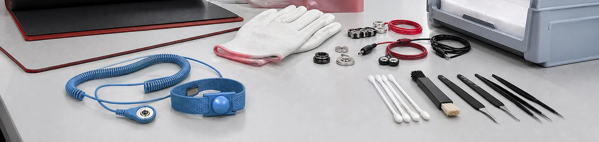
ESD Trays & JEDEC IC Trays
Source ESD trays for components, PCBs and semiconductor packages used in assembly, inspection and storage. Quandun’s range includes open component trays, divided trays and JEDEC-style IC carriers. Compare the part envelope, support geometry and pocket layout before selecting a format for bulk or repeat supply.
-
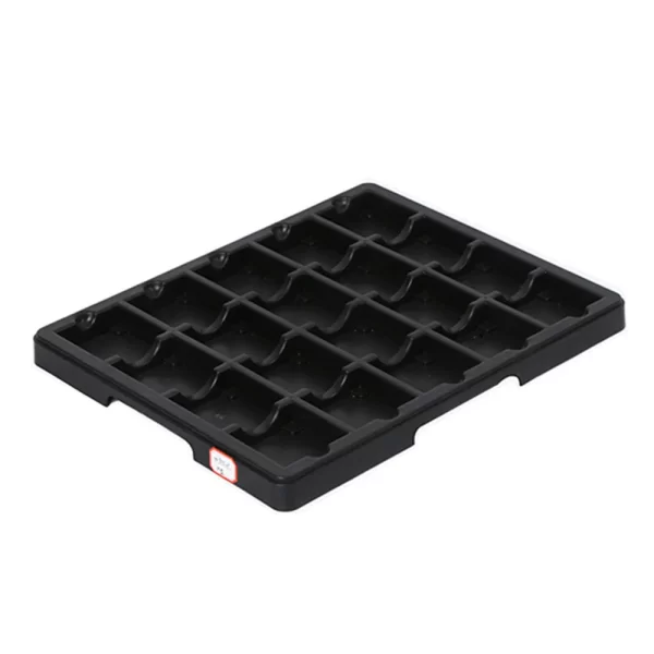
Detachable Grid ESD Tray
-
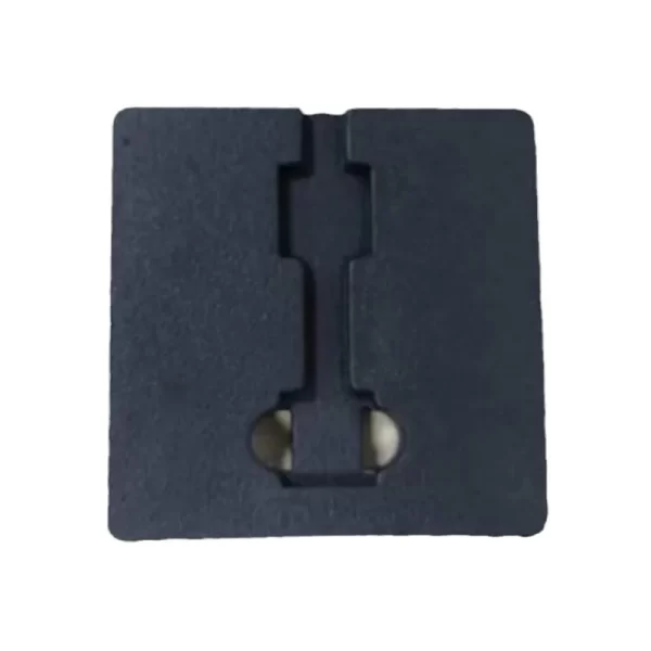
EVA Rubber Integrated Molding Tray
-
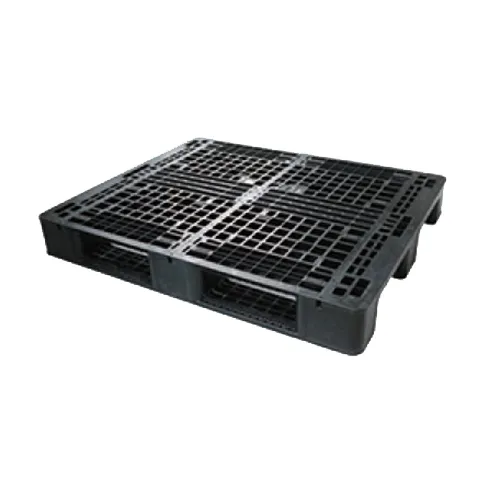
Heavy-Duty ESD Pallet
-
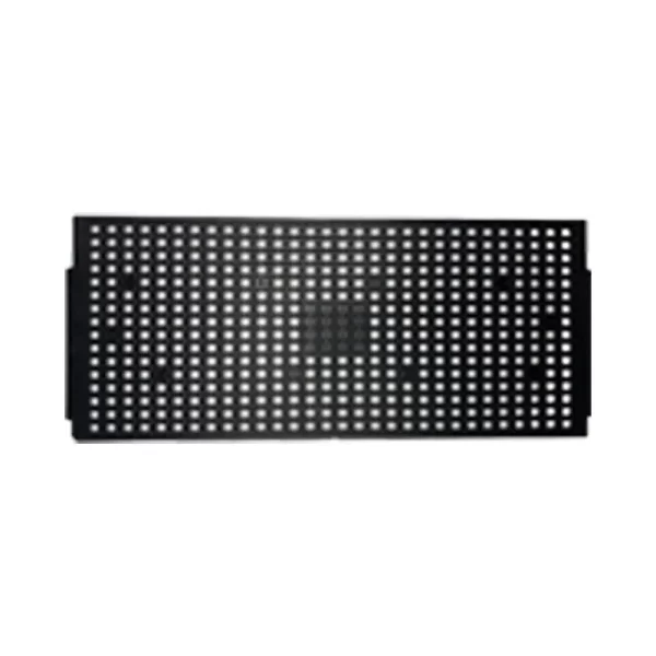
JEDEC Standard ESD IC Tray
-
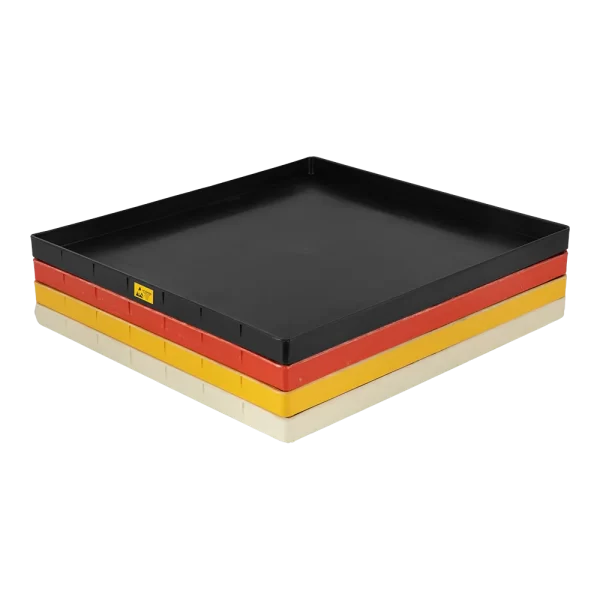
Multi-cavity ESD Tray
Choose the tray format for the component
| Format | Published example | Selection check |
|---|---|---|
| Component tray | QD-9805108: 225 × 165 × 37 mm outside; 215 × 155 × 32 mm inside | Check the packaged part, removal clearance and support surface. |
| Detachable grid tray | QD-9805112: 457 × 312 × 39 mm outside; 417 × 292 × 30 mm inside | The listing identifies 70 detachable compartments; request the assembled cell layout. |
| IC matrix tray | BGA6x8 / EA70608-10: 16 × 30 matrix, 480 positions | Confirm the exact IC package and pocket drawing; a matrix count alone does not prove fit. |
These are examples from the linked specification tables. Whole-tray inner dimensions are not the usable dimensions of every compartment. The IC tray model name is not a substitute for a pocket drawing or device compatibility check.
Compare component tray height as well as footprint
The component tray specification lists QD-9805108 at 215 × 155 × 32 mm inside and QD-9805110 at 275 × 185 × 23 mm inside. The second has a larger inside plan area but less listed height. A wider tray is therefore not automatically suitable for a taller assembly. Check the complete loaded part envelope and support arrangement against the selected drawing.
For sample approval, confirm where the part touches the tray, whether fingers or a handling tool can remove it, and whether a cover or the tray above can contact a connector or component. For the 70-compartment QD-9805112, use a cell drawing rather than dividing the whole-tray dimensions by the number of cells. Record the approved layout and part orientation with the order.
How to specify ESD trays for PCB and SMT components
Provide the component outline, package state, sensitive contact areas, quantity per tray and loading orientation. Identify the intended support points so a lead, connector or tall component does not become the load-bearing surface. Check removal access, neighboring parts, the cover and the underside of the next tray when stacked.
For a tray with dividers, state the largest packaged part and the space needed to grasp it. For semiconductor handling, identify the BGA or QFN package and the required carrier drawing. Compare the kitting tray guide for mixed assemblies and the divider selection guide for compartment planning.
Thermoformed, molded and heat-resistant are different requirements
A cavity photograph does not establish the manufacturing process. If your specification requires a thermoformed ESD tray, state that process, material, sheet thickness and tooling requirement explicitly. The thermoformed tray guide separates those questions from general tray geometry. Confirm time and temperature for any heating step rather than applying one model’s option to the entire range.
Check storage, cart and shipping interfaces
Measure the loaded tray, including protruding components, covers and labels. A cart needs a supporting shelf or rails with suitable clearance; PCB edge slots do not automatically support a tray. Use the ESD tray cart guide to define that interface. Where the tray leaves an ESD protected area, use the ESD shipping-container guide to specify the complete protective package separately. A tray supports the load; it does not by itself establish shielding for shipment.
Request ESD trays for a production or packaging project
Use the ESD meaning and material distinctions when specifying the required electrical evidence. For a deeper outer container rather than a presentation tray, compare ESD boxes.
Send the part drawing, proposed quantity per tray, loading direction, stack arrangement and order quantity. For a JEDEC-style IC carrier, include the exact device package and required pocket drawing. Identify heat exposure or machine-interface requirements separately; the selected model must support them.
Request a quotation with the relevant tray link. For a requested size or layout change, review OEM and ODM capability and confirm the model-specific scope, drawing and sample requirements before ordering.
Contact Us
Quandun has developed into a professional enterprise integrating scientific research, industrial manufacturing, international trade, engineering design and technical training in the field of electrostatic environmental protection.
Address
No.320 Kaichuang Rd, Baitawang Community,Beibaixiang Town, Yueqing, Wenzhou, Zhejiang, 325603, China
Hours
Monday~Sunday: 8am to 8pm