


An NPN vs PNP transistor comparison starts with opposite BJT polarity. In normal forward-active operation, an NPN base is positive relative to its emitter and conventional collector-path current runs from collector to emitter. A PNP reverses those relationships: its base is negative relative to its emitter and conventional current runs from emitter to collector.
That difference explains the symbols and common switching positions, but it does not approve a component substitution. Package appearance, lead order, current gain and operating limits still need separate checks. This guide connects the basic polarity comparison to a practical component-selection record for electronics purchasing and assembly teams.
NPN vs PNP transistor: the key structural difference
NPN and PNP are types of bipolar junction transistor, or BJT. An NPN structure has a P-type base between N-type regions. A PNP has an N-type base between P-type regions. Both have three functional terminals: base, collector and emitter. Reversing the semiconductor types changes the normal polarity and current relationships.
| Comparison | NPN BJT | PNP BJT |
|---|---|---|
| Structure | P-type base between N-type regions | N-type base between P-type regions |
| Base relative to emitter in normal forward-active operation | Positive | Negative |
| Conventional collector-path current | Collector to emitter | Emitter to collector |
| Emitter arrow in the schematic symbol | Points outward | Points inward |
| What the name does not specify | Package lead order or complete ratings | Package lead order or complete ratings |
The table describes normal functional relationships, not every possible operating condition. It should help a reader interpret a schematic and ask better data-sheet questions. It is not a universal wiring instruction or a claim that every NPN device is interchangeable with another NPN device.
ROHM’s transistor overview and Toshiba’s BJT learning material explain these basic distinctions. For a real selection, move from the generic type to the exact manufacturer part number and package drawing. A catalog description containing only “NPN transistor” leaves most of the information needed for an approved purchase unresolved.
Read polarity relative to the emitter
The phrase “negative base” can be misleading if the reference is omitted. For a PNP transistor, it means negative relative to the emitter in the stated operating context. It does not automatically mean the circuit requires a negative supply relative to ground. Voltage is a difference between points, so the reference must remain explicit.
Use the notation VBE to keep that reference visible: base potential minus emitter potential. The sign of that difference helps distinguish the polarity discussion from a statement about the whole power supply. This is particularly useful when a diagram places a PNP emitter near a positive rail and the reader assumes that every transistor terminal must then be described as simply positive.
The generic comparison does not establish a universal base-emitter voltage. The actual relationship depends on the device and operating conditions. Do not turn a familiar approximate value from a teaching example into a guaranteed turn-on threshold for a purchasing specification or a design review. The relevant manufacturer curves and stated test conditions control that assessment.
In a component discussion, ask two separate questions: which terminal is the reference, and under what operating condition is the value specified? This prevents a correct sign convention from being mistaken for a complete drive requirement. It also helps distinguish a misunderstanding of the schematic from an actual mismatch in the selected device.
Symbols and conventional current direction
The emitter arrow points outward for an NPN symbol and inward for a PNP symbol. It is a polarity aid within the schematic, not a drawing of the physical lead positions. Rotating or mirroring a schematic symbol does not change the manufacturer’s package pin assignment, which must be read from the actual device documentation.
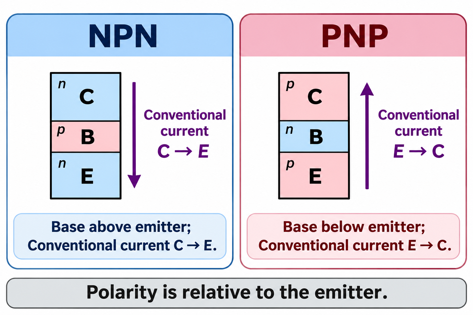
Conventional current direction also needs to be distinguished from the motion of charge carriers discussed in semiconductor explanations. A drawing of electron motion should not be combined with a conventional-current arrow without identifying which convention each arrow uses. The comparison in this article consistently uses conventional collector-path current.
For an incoming component check, preserve the exact package-view convention. A drawing may identify a top view or another orientation. Reading it from the wrong side can reverse the apparent lead order even when the part number is correct. The schematic symbol alone cannot resolve that physical orientation question.
A practical review therefore keeps three items separate: functional symbol, electrical terminal names and physical package drawing. Matching only one of them is insufficient. When a proposed substitute arrives in an identical-looking package, compare the actual terminal assignment rather than using the external silhouette as evidence of electrical equivalence.
Low-side and high-side describe circuit position
An NPN transistor is commonly explained in a low-side switching role, while a PNP is often introduced in a high-side role. These descriptions concern where the switching device sits relative to the load and supply references in the illustrated topology. They do not mean that the polarity name alone defines every possible circuit arrangement.
ROHM’s low-side fundamentals provide context for the common-emitter NPN example. For a buyer reading a specification, the useful distinction is between the transistor’s device type and the behavior required by the complete circuit. A circuit-position label cannot replace checks of voltage, current, drive, thermal conditions and the approved schematic.
Also avoid transferring the names directly to industrial sensor compatibility. A product described as an NPN or PNP output has a broader interface specification. Its supply requirements, output arrangement and receiving input must be considered together. A bare-transistor polarity comparison is not a complete sensor or control-system compatibility guide.
If a proposed replacement changes polarity, stop treating it as a package-equivalent swap. The circuit relationships need a separate engineering review. Even when polarity stays the same, the replacement may still differ in limits or behavior. Procurement can collect the exact documentation and identify the proposed change; the name “NPN” cannot approve it on its own.
Current gain is conditional, not a fixed multiplier
In a simplified forward-active explanation, collector current is related to base current through current gain. Toshiba expresses this relationship using hFE. The value belongs with its stated operating conditions. A data-sheet number should not be treated as a constant that applies across all currents, temperatures and operating regions.
For a hypothetical forward-active gain of 100 and base current of 20 µA, the illustrative collector current is 100 × 20 µA = 2,000 µA, or 2 mA. These are teaching inputs, not ratings for a supplied part. The arithmetic does not establish a saturation condition, a suitable load or a safe drive circuit.
If another hypothetical device has a different gain, that does not make it a universally better replacement. The circuit task determines which characteristics matter, and gain must be assessed with the conditions under which it is specified. A comparison using one device’s typical value and another device’s minimum value can be misleading even when the numbers look easy to rank.
In a selection sheet, give the parameter, value type and test conditions separate fields. Preserve whether the source specifies a minimum, typical value or range. Do not replace a range with an invented midpoint. This keeps an apparently precise calculation from concealing the fact that the source values were not equivalent or did not apply to the intended operating region.
Compare data sheets instead of matching packages
The approved manufacturer part number is the starting point for a controlled comparison. The package suffix, documentation revision and assembly requirement may matter as well. A short marking on the device can help with identification, but should not be interpreted as a complete cross-reference without manufacturer support.
| Selection check | Evidence to compare | Why appearance is insufficient |
|---|---|---|
| Device class and polarity | BJT type and NPN or PNP designation | Other three-terminal devices can look similar |
| Terminal assignment | Manufacturer package drawing and view orientation | Lead order is not universal |
| Electrical limits | The relevant rated quantities and their conditions | One headline current value does not define the application |
| Gain and switching behavior | Specified parameters under comparable conditions | Values vary with the operating point and test basis |
| Thermal conditions | Applicable thermal information for the actual arrangement | Package shape alone does not establish heat removal |
| Assembly fit | Footprint, body envelope and lead geometry | A visually similar part may not match the controlled footprint |
| Approval status | Documented engineering disposition | A distributor description is not substitution authorization |
Use a comparison table to expose differences, not to prove equivalence by counting matching fields. One unresolved requirement can be decisive for the application. If a field is absent from a supplier summary, request the actual data sheet rather than assuming the original and proposed parts share it.
The disposition should identify what was approved and for which assembly revision. “Equivalent transistor” without a defined reference can become ambiguous later when the circuit or approved source changes. A controlled record allows receiving inspection, production and purchasing to refer to the same decision instead of relying on a remembered conversation.
Keep component identity through storage and assembly
Correct selection can be undermined if the components lose their identity before assembly. Keep the manufacturer part number, approved source, lot information and intended assembly reference associated with the physical stock. Do not mix a proposed substitute with approved inventory merely because both devices have three leads and similar bodies.
| Handoff field | Example of the information type to retain | Question it answers |
|---|---|---|
| Component identity | Full part number and package suffix | Which exact device is present? |
| Documentation | Data-sheet reference and approval record | Which evidence supports its use? |
| Inventory identity | Lot or receiving reference | Which stock does the record describe? |
| Assembly destination | Board revision and fitted option | Where is this component approved to go? |
| Handling requirement | Applicable component and site controls | How must it be protected before assembly? |
Select carriers around the actual package and handling requirements. ESD trays for component handling can be considered as part of that route, with fit and material evidence checked for the proposed configuration. A tray does not establish transistor compatibility, confirm a pin assignment or authorize a substitution.
EOS/ESD Association guidance provides broader handling context for sensitive electronics. Apply the device documentation and the site’s approved controls rather than assuming every BJT has the same sensitivity or packaging requirement. Keeping identity, electrical approval and handling evidence connected supports a more reliable assembly handoff without confusing those three separate decisions.
Questions about NPN and PNP selection
Can a PNP transistor replace an NPN if the package matches?
Package fit does not reverse the required polarity or circuit relationships. A change from NPN to PNP requires engineering assessment of the circuit, not a lead-for-lead purchasing substitution. Even devices of the same polarity need their actual pin assignments, operating characteristics and approval status compared before replacement.
Is a transistor with higher gain always preferable?
No. Gain is one conditional characteristic within a larger application. A higher listed value may have been measured under different conditions and may not address the circuit’s limiting requirement. Compare the relevant minimum, typical or range information on a common basis, then assess it against the actual design task rather than choosing the largest number.