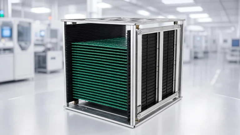


A dual inline package is an electronic component package with two parallel rows of leads. DIP is the usual abbreviation; dual in-line is another common spelling. In the familiar through-hole form, the leads enter a circuit-board footprint or a compatible socket. The package describes the physical format, not what the circuit inside does.
That distinction is the most useful part of dual inline package meaning. Two devices can both be DIP packages and still have different dimensions, pin functions or operating limits. Identifying the package is the start of a component check. It is not evidence that a replacement is electrically equivalent or that a storage carrier will support the part correctly.
Dual inline package meaning: DIP, DIL, PDIP and CDIP
Texas Instruments describes DIP packages as dual-row formats with leads on two parallel sides, available in plastic and ceramic constructions. The familiar outline makes individual leads visible and provides a clear mechanical interface. A component can be soldered into an appropriate through-hole board or used with a socket that matches the particular package.
| Label | What it helps identify | What still needs checking |
|---|---|---|
| DIP / dual in-line | Two parallel lead rows in the package family | Pin count, outline and device specification |
| DIL | Another dual-in-line description in component usage | The actual manufacturer package designation |
| PDIP | Plastic dual in-line construction | Exact package drawing and ordering suffix |
| CDIP | Ceramic dual in-line construction | Exact outline and device-specific conditions |
Treat prefixes and suffixes as a route to the manufacturer’s documents. They can distinguish package options within one device family, but they do not replace the complete ordering code. In a purchasing record, keep the device identifier and package designation together. A description such as eight-pin DIP is too broad to define a complete interchangeable component.
Read pin numbering from the view named in the drawing
Pin orientation begins with the manufacturer’s pin-one identification and the view shown in the document. A top view and a view from the underside are not interchangeable. A notch, dot or other index feature helps establish orientation, but the specific drawing determines how that feature relates to the pin numbers.
In the generic eight-pin top view shown below, the notch is at the top. The left row runs from 1 at the upper left to 4 at the lower left. The right row runs from 8 at the upper right to 5 at the lower right. This explains the numbering relationship; it does not assign power, ground or signal functions to any pin.
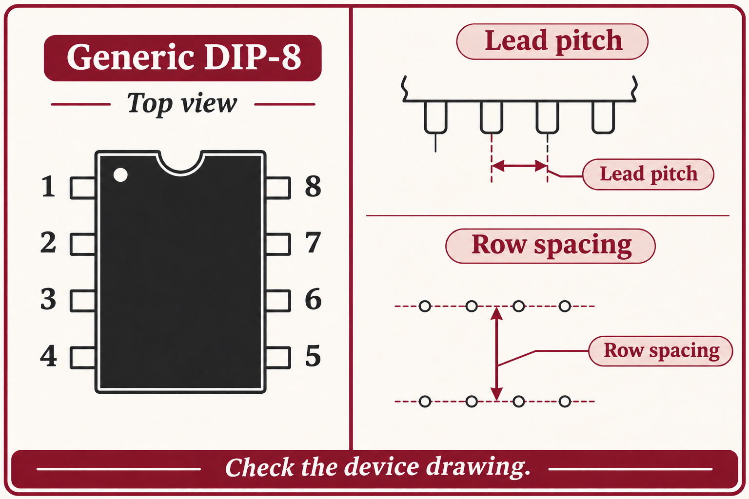
The package outline and the electrical pinout answer different questions. The outline locates the leads. The pinout tells the reader what each lead does for that device. A socket can accept the physical leads while connecting them to an unsuitable circuit. Keep both documents available when reviewing a replacement instead of using the package photograph as the only reference.
A useful orientation check records the view, index feature and first pin before anyone compares the remaining pin functions. If a sketch or supplier photograph does not state its view, return to the controlled drawing. Rotating a photograph until it resembles a footprint is not a dependable way to establish the pin assignment.
The dimensions that determine footprint and socket fit
Several different distances can look like package width in a photograph. Body width describes the molded or ceramic body. Row spacing describes the relationship between the two lead rows. The overall lead envelope includes the projecting leads. Lead pitch is the repeated spacing along a row. These dimensions affect different mechanical checks and should not be copied into the same field.
| Drawing item | Decision it supports | Common interpretation error |
|---|---|---|
| Pin count and pitch | Number and spacing of positions along the footprint | Assuming every package with the same count has the same pitch |
| Row spacing | Distance between the two lead rows | Measuring body width or the visible gap between lead tips instead |
| Body and lead envelope | Clearance around the complete part | Using only the black body silhouette |
| Height and seating information | Space above the board and intended seating relationship | Ignoring socket height or nearby hardware |
| Lead dimensions and tolerances | Fit with the specified footprint or socket | Treating a single nominal distance as the whole tolerance requirement |
Microchip’s PDIP drawing separates top, side and end views and labels the relevant body and lead dimensions. That separation is useful even when no actual dimensions are copied into a general guide. It shows why a purchasing sketch should identify the dimension being requested and why a package photo cannot supply a complete mechanical specification.
Compare dimensions using the same definitions and units. If one source gives a body dimension and another gives a distance across leads, the values are not competing answers to the same question. Record which drawing controls the purchase, its revision and the required footprint or socket. Resolve a difference in the documents before accepting an apparently close visual match.
DIP versus a surface-mount package
A familiar DIP through-hole format and a surface-mount package create different board interfaces. Choosing between them affects the footprint, handling and assembly route. It is not simply a choice of which component looks smaller. A device family may have more than one package option, and the ordering code must identify the intended one.
For prototyping, socketing or breadboard work, the accessible lead arrangement can be convenient. For a production assembly, the team must still evaluate its actual board and manufacturing process. Do not turn a general description of package convenience into a rule that DIP is always more durable, more accurate or electrically superior to a surface-mount alternative.
A proposed package change also changes the review questions. Is the same device offered in the new package? Does the pinout stay the same? Has the board footprint changed? Is a different assembly process required? Keeping those questions separate helps a buyer explain why an alternative package needs engineering approval even when the device name appears familiar.
Why matching DIP packages do not prove replacement compatibility
Mechanical compatibility is only one part of replacement. The function, pin assignments, supply conditions and operating limits belong to the selected device’s data sheet. A family name or a common number of leads does not establish those properties. TI data sheets illustrate the need to read device information alongside the package options.
| Review layer | Question to answer | Evidence to retain |
|---|---|---|
| Identity | Is this the intended device and ordering option? | Complete manufacturer part number and supplier record |
| Mechanical | Does the exact outline match the board or socket? | Controlled package drawing and footprint reference |
| Electrical | Do functions, pin assignments and operating limits match? | Device data sheet and engineering approval |
| Process | Can the chosen assembly and handling route support it? | Applicable assembly requirements and carrier decision |
This matrix is also useful when a supplier proposes an alternative. Asking only whether an alternative is DIP-compatible leaves the meaning unclear. Ask which layer has been compared. A proposed part may pass the outline comparison while its electrical review remains incomplete. That is a precise unresolved decision, not a reason to improvise a substitution on the bench.
The same principle applies to sockets and carriers. A socket is an electrical and mechanical interface with its own intended package range. A tray is a handling support. Neither creates electrical equivalence between components. A generic storage compartment should not be described as a compatible IC socket, and a JEDEC-style tray label alone does not demonstrate fit for a DIP device.
Inspect the package without confusing appearance and performance
For incoming inspection, separate visible condition from functional acceptance. The label and ordering code establish the claimed identity; the package drawing supports the outline check; visible lead condition informs the handling decision. A clean appearance does not prove electrical performance, while an unclear marking is a reason to resolve identity rather than guess from a similar package.
For storage and movement, account for the projecting leads as part of the complete envelope. Plan the support surface and removal access so the handling arrangement does not rely on delicate leads carrying an unintended load. A drawing of the loaded part is more useful than a body-only length and width when comparing compartments, lids or a stack of trays.
CH-ESD’s ESD component trays provide a starting point for that handling comparison. Match the actual part, support geometry and access requirements to the selected carrier. A category name does not confirm DIP compatibility. For sensitive devices, the required electrostatic controls and packaging properties should come from the applicable handling program and component information.
A practical carrier review asks what touches the component, what prevents neighboring parts from contacting one another, and how the part is removed. It then checks the assembled arrangement, including any cover or divider. This makes the handling requirement visible before the order is reduced to a tray size or a black-plastic description.
Package information to keep with an order or alternative-part request
A concise package record includes the complete device number, manufacturer package designation, pin count, controlling drawing and revision, named drawing view, relevant outline dimensions and intended footprint or socket. Add the handling state: loose component, individually protected part or populated assembly. Those states can lead to different carrier requirements.
For a proposed alternative, attach the mechanical comparison and identify the separate electrical approval. For a carrier purchase, attach the actual part envelope and explain the support and access task instead. These are different requests, even when both begin with the same DIP package name. The supplier should be able to see which decision it is being asked to support.
FAQ
Does DIP identify the circuit function?
No. DIP names the package family. The complete device identifier and data sheet establish its function, pin assignments and operating limits. Two visually similar DIP components can perform different jobs.
Can a package photograph replace the outline drawing?
A photograph can help identify visible features, but it does not supply controlled dimensions, tolerances or a defined drawing view. Use the manufacturer’s package drawing for a footprint or socket comparison, and retain the device data sheet for electrical checks.
References
- Texas Instruments DIP package family — dual-row construction, package variants and dimensional filters.
- Microchip PDIP outline — separate top, side and end views and outline dimensions.
- Texas Instruments device data sheet — example of device-specific electrical information and package options.
- EOS/ESD Association fundamentals — electrostatic-sensitive-device handling and packaging context.