
Laser direct imaging (LDI) transfers a digital pattern onto photosensitive material using a laser to expose the pattern, without the conventional film phototool used for that exposure. In PCB fabrication, this helps connect the approved manufacturing data to the pattern on a panel. It does not mean that a laser cuts every copper trace out of a finished board.
The useful question for a buyer is where LDI is used and what the fabricator can demonstrate on the specified material. An equipment name alone does not establish finished line width, registration, yield or electrical reliability.
Where laser direct imaging fits in PCB manufacturing
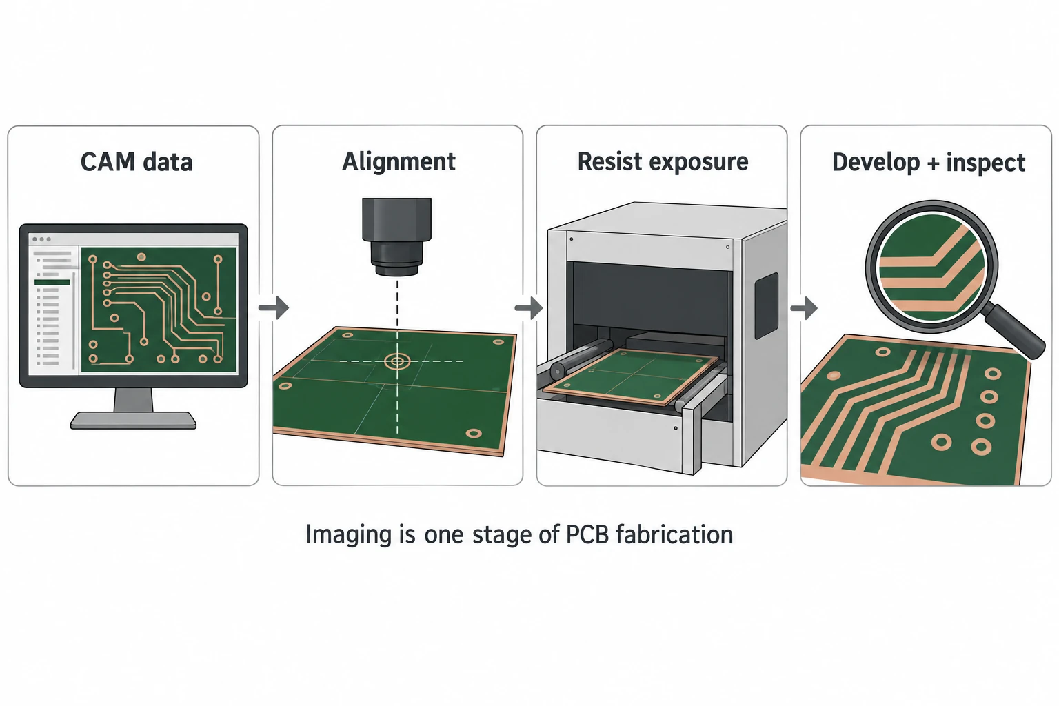
A resist-patterning route includes preparing a photosensitive layer, aligning the panel, exposing the required image and developing that layer. The resulting pattern participates in subsequent processing. The precise sequence depends on the fabrication route; the exposure machine is one part of it.
Digital data still needs manufacturing preparation. Computer-aided manufacturing (CAM) establishes the production representation of the design, while alignment relates that representation to the actual panel. KLA describes CAM connectivity, target acquisition and scaling modes for its direct-imaging equipment. Those functions show why image transfer involves more than loading a picture and pressing a button.
Direct imaging can also be used for solder mask. Limata lists both resist patterning and solder-mask imaging among its applications. The exposed material and the purpose of its pattern differ, so a fabricator’s statement that it uses direct imaging should identify the relevant stage.
LDI, phototools and laser ablation are different
| Term | Role | Question to ask |
|---|---|---|
| Film phototool exposure | A physical pattern controls exposure of photosensitive material | How is the tool version and registration controlled? |
| Laser direct imaging | Digital data controls exposure without that film tool | Which resist or solder mask and which process stage? |
| Laser material removal | Material is removed rather than merely exposing a light-sensitive layer | What material is removed and how is the result checked? |
“Direct” describes the imaging route, not the elimination of all downstream work. A well-defined comparison keeps the exposure method separate from development, copper processing and final inspection. It also avoids treating every process that contains a laser as LDI.
What digital exposure can change
Removing the film phototool from the exposure step changes how design revisions reach production. The manufacturer still needs to identify the approved data version, preserve the intended pattern and control registration. Replacing physical artwork with digital data does not remove revision-control responsibility.
M&R describes maskless exposure using optical scanning, motion control, alignment and focus functions. These explain the flexibility of the approach. They are not permission to apply one machine’s resolution specification to a different resist, panel or production line.
For the same reason, a supplier’s quoted machine throughput should not be treated as the turnaround time of an entire PCB order. Exposure time is only one operation. Other process stages and the verification required for the particular board still matter.
A more useful way to verify an LDI claim
Ask for a short process record tied to the intended board. Four entries make a claim easier to evaluate without demanding a machine demonstration that says little about the order:
- Stage and material: state whether imaging concerns resist or solder mask, and identify the material system.
- Design and revision: identify the released manufacturing data and how changes are controlled.
- Required feature: distinguish the nominal design feature from the acceptance limit on the processed board.
- Verification: identify the inspection or measurement that demonstrates the required result on the relevant output.
For example, a fine-line design question and a solder-mask registration question require different evidence. Combining both under “high-precision LDI” leaves the actual requirement unresolved. Keep the requested feature, material and evidence together.
Keep imaging performance separate from board handling
After fabrication and during assembly, the board may require support that avoids contact with components or vulnerable features. Quan Dun’s ESD trays can be assessed for that handling task against the real assembly dimensions and contact points. The tray is not evidence of the fabricator’s imaging capability.
A sensible production discussion therefore keeps two records: how the board’s features are produced and verified, and how the resulting board or assembly is handled. That distinction makes an LDI claim useful without turning it into a promise about every later operation.