

One of the hidden enemies in the field of Printed Circuit Boards is Electrostatic Discharge or ESD. It is essential that one understands ESD for PCB and knows how to protect his circuit so that electronic devices can serve a prolonged life. The article covers the definition of ESD, its consequences for PCBs, and recommendations for implementing ESD protection in the design.
Understanding ESD and Its Effects on PCB
ESD stands for when electricity flows from one charged device to another, usually due to physical contact, a short circuit, or dielectric failure. The flow of electricity leads to damaging effects on the electronics with possibly severe consequences for sensitive parts of circuits. Hence cases of ESD could lead to malfunctioning and therefore unreliable electronic devices and expensive repairs because the effects of ESD could either be immediate or latent.
How to Protect PCB from ESD?
To protect a PCB against ESD, several important steps must be taken. The most important factor is ensuring that both the work area and workers are properly grounded. Here are some techniques used to provide ESD protection to PCB:
1. Grounding:Confirm that all gear and people who come into contact with the PCB are in good shape with regard to grounding. This practice appreciably reduces the probability of ESD occurrences.
2. Electrostatic Discharge Safe Workstation:Use ESD-safe surfaces and wrist straps to minimize charge build-up.
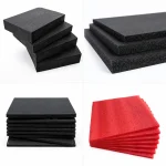
3. Handling ESD-safe Components:Use containers ,storage racks and bags that ensure safe handling, storage, and shipping of components.
4. Design Considerations:Include the use of spark gaps and ESD protection components directly on PCB for the purpose of absorbing discharge voltages and ensuring the safety of delicate circuitry.

Additional Tips for ESD PCB Design
Although the measures mentioned above are significant, the incorporation of ESD protection while designing your PCB can cause a huge impact. Here are some related tips:
1. Implement Ground Planes:Incorporate broad ground planes in the design to aid in carrying away ESD energy from vulnerable traces.
2. Strategic Location of Components: Position sensitive components far from any discharge entry points which include connector pins.
3. The Use of ESD Suppressive Devices: Employ these devices as suppressors and filters that absorb the voltage and lead the current of ESD to ground.
FAQ: Common Concerns About ESD PCB
Q: How to protect PCB from ESD?
In order to safeguard the PCB from ESD, make sure the entire system and work stations are properly grounded, make use of ESD-safe materials, and incorporate protective elements such as ESD suppressors in the PCB design.
The Importance of ESD Awareness
Incorporating knowledge about ESD and proper protection methodologies into the design and assembly process of PCBs is essential. Not only does it stop the damage from happening right away but also improve product reliability, raise consumer confidence, and possibly reduce the return rates of electronic goods.
To wrap things up, it is extremely important to deal with and design PCBs with ESD aware. If you follow the right methods, you will get to protect your circuits, achieve better performances, and prolong product life cycle making sure your electronic products stay functional and reliable in competitive conditions of modern market.